


Database "Bandgap"
The Bandgaps (Forbidden Zones) of Solids (Semiconductors, Dielectrics & Semimetals)
Cite us
If you use "Bandgap" DB in a scientific publication, we would appreciate citations to the following paper:
Kiselyova N.N., Dudarev V. A., Korzhuev M. A. Database on bandgaps of inorganic substances and materials // Inorganic Materials: Applied Research. 2016. V. 7. № 1. P.34-39.
(https://doi.org/10.1134/S2075113316010093)
Introduction
The concept of forbidden zone Eg (or an energy gap in electronic spectrum of crystals ΔE) was formed by the solid state physics during the explanation of distinctions between physical properties of metals and insulators (dielectrics) within the framework of quantum physics [1-4]. According to quantum theory the number of final electronic states in a crystal precisely corresponds to the number of initial states in atoms forming it [4]. In addition for quantum system W.Pauli's exclusion principle only 2 electrons with opposite spins may settle down at each energy level. So at the formation of a crystal from separate atoms owing to reduction of inter nuclear distances electronic levels of atoms transforms into quasiunbroken allowed zones (bands) having certain width on energy scale.
The width of allowed zones depends on energy of connection of electrons with a nucleus of atom. The allowed zones of a crystal are separated from each other by forbidden zones, the density of electronic states in which is equal to zero [1-6].
The electrons fill in only the allowed zones, the electrons may not settle down in the forbidden zones of an ideal crystal [2,3]. The concept of E.Fermi energy (level) EF, separating the filled electronic states of a crystal from free ones at zero absolute temperature (T = 0 K), is used for the characteristic of filling of electronic zones by electrons.
Accordingly to position of EF on energy scale the allowed zones of a crystal may be filled by electrons completely, partially, or remain vacant one. The top zone from the all filled zones refers to as valence band, the bottom zone from the all of vacant zones - the conductive one [3].
The arrangement of Fermi level EF concerning the edges of the bands mentioned above determines an electronic nature and physical properties of a crystal. Really, the valence electrons of a crystal, taking place in the fully filled bands, are fixed and do not participate in conductivity. The electrons may become mobile and participate in electronic conductivity only if they are in the partially vacant zone [4]. So substances, in which the valence band is filled partially, or conductive and valence bands are crossed over, are metals (in addition electrons should not be located as in some narrow band semiconductors with strong electron bonding). Substances, in which at zero absolute temperature (T = 0 K) the valence band is filled (or nearly so filled), and a conductive band is empty (or nearly so empty), and the last are not crossed, are semiconductors or dielectrics (insulators) [3,4].
Dynamic characteristics of electrons in bands are determined by dependence of their energy E on impulse p = (h/2π)k (here k is wave vector). Usually dispersal curves E = f(p) near the band edges are described by square-law dependence:

(here h is M.Planck constant, ki are spatial components of a wave vector, m is effective mass of electrons). Such curves get more complex view if they are far from extreme [5,6]. The band structure of a crystal in coordinates E-k represents as a set of dispersal curves, energy gaps between which vary from point to point in impulse space [6]. The spatial periodicity of a crystal determines the periodicity of impulse (speed) space of electrons also. That allows allocation of the elementary cell in impulse space named as Brillouin zone of a crystal. The form of Brillouin zone is determined by symmetry of a crystal, thus energy extreme on dispersal curves are usually located in symmetric points of Brillouin zone (L, X, Δ, Γ and others).
Forbidden zone Eg and chemical bonds in solids
The nature of chemical bonds in solids is determined by the minimal energy gap between an absolute maximum of a valence zone and an absolute minimum of a zone of conductivity which is named as the fundamental forbidden gap, or simply forbidden gap of crystal - Eg [1,5]. Depending on, whether extreme of conductivity and a valence bands locate - in the same points of Brillouin zone, or are separated in impulse space, Eg is referred to as direct or indirect [4,5].
Semiconductors and dielectrics distinguish on Eg size. By convention substances with Eg > 2-3 eV (1 eV = 1.6021*10-12 erg = 1.6021*10-19 J) belong to a class of dielectrics (insulators), substances with Eg < 2-3 eV - to a class of semiconductors (1.5 eV < Eg < 2-3 eV - to a class of wide-bandgap semiconductors, Eg < 0.1-0.2 eV - narrow-bandgap semiconductors). Substances with Eg ≈ 0 belong to a class of zero-bandgap semiconductors, substance with Eg ≤ 0 (small overlapping of zones) - to a class semimetals. High doped semiconductors with metallic character of conductivity, in which EF is located deeply in conductivity, or valence zones, belong to semimetals also [5,7]. One should distinguish the narrow-bandgap semiconductors and the narrow band semiconductors, the last are referred to as when allowed zone range is narrow (< koT) [7].
The concept of Eg may be extended to disordered and strongly defective phases, including on amorphous substances (glasses) [8,9], and also liquids [10], where the role of Eg plays pseudo gap Eg*. The last represents an energy gap, within which both the located and the widespread electronic states may be present.
The concept of Eg loses their meaning for gaseous dielectric phases (at least for no ultrahigh pressure), being transformed into usual energy gaps between the occupied and free energy levels of electrons in atoms or molecules.
Thus, Eg is the basic parameter of the condensed matter, which characterizes a nature of chemical bonds and accordingly determines the chemical, physical-chemical and physical properties of solids.
Eg and other parameters of solids
Eg in solids is defined by a nature of chemical bonds, composition of a compound, its deviation from stoichiometry, aggregative state, crystal and, in some degree, defective structures of a sample. The size of Eg depends also on temperature, pressure, electric, magnetic, gravitational fields and other external parameters [1-11]. As a rule, the linear factors (e.g., temperature αT = δEg/dT and pressure - αP = δEg/dP coefficients, here T and P are absolute temperature and hydrostatic pressure) are used for the description of these dependences. Sometimes (e.g., at phase transitions) factors of higher order may be used. At change of composition, a deviation from stoichiometry (phases of variable composition), and also of some external parameters (temperature, pressure, etc.) structural or electronic phase transitions of semiconductor-dielectric or semiconductor-metal associated with Eg change can be observed [12]. The last can be described by the general ratio:
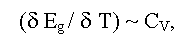
(here Cv is a thermal capacity at constant volume). Accordingly, Eg curves drops near a phase transitions of first order and have a bent near a phase transitions of second order similar to Cv curves [17].
The type of the chemical bonds of compound, the stability of compounds in the certain interval of changes of composition and external parameters, the type of electronic conductivity, the possibility of ionic conductivity in samples, and also the basic thermodynamic characteristics of bonding in solids (enthalpy of formation HF, entropy ΔSm, melting point Tm, etc.) could be inferred by the value of Eg [13].
The influence of Eg value on electrical and optical properties of samples is most strongly expressed in intrinsic materials (Fermi level EF lies in the forbidden zone). In doped semiconductors EF lies in a valence or in a conductivity zones, so the influence of Eg value on physical properties of crystals weakens and at EF 5-10 koT > Eg becomes practically imperceptible. The last is valid also for conductivity over deep d-bands in the semiconductors, containing transition metals.
Methods of Eg determination
Now experimental and theoretical methods of research of band structure of solids cover an energy up to ~25 eV [16]. The methods of the quantum theory (a linear combination of atomic orbitals, orthogonalised plane waves, pseudo-potential, etc.) are used for theoretical calculations of band structure. The accuracy of theoretical calculations of Eg usually does not exceed ~ 0.5 eV. The accuracy of theoretical calculations, however, may be raised by use in some support experimental points [16]. Now the good qualitative understanding of a band structure in a wide energy interval, and in some cases semi-quantitative knowledge of band structures in an interval 10-20 eV (accuracy may reach 0.5-1.0 eV) for many solids is achieved [16]. At the same time, theoretical calculations of band structure of solids are still too rough in order to interpret unequivocally, for example, spectra of electrical reflection (the experimental resolution of spectral peaks exceeds ≈0.01-0.001 eV) or to predict the gaps between valence and conductive zones where required accuracy is more than ≈0.1 eV [16]. Therefore now reliable determination of Eg is based on the experimental methods which accuracy exceeds ≈0.1 - 0.01 eV [15,16].
Eg value is determined experimentally from the analysis of the various physical effects associated with electron transitions from valence to conductive zones under thermal activation (Egterm), or quantum of light (Egopt). Usually Egterm is obtained from a temperature dependence of electrical resistance ρ and/or Hall factor R for intrinsic conductivity, and Egopt - from band edge of absorption and longwave boundary of photo-conductivity. The Eg value can be estimated also from measurements of a magnetic susceptibility, heat conductivity (bipolar component), some experiments on tunneling at low temperature, etc. [15]. There are also some empirical equations for quality evaluations of width of forbidden zone Eg, for example:
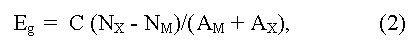
(here NX, M and AX, M are the number of valence electrons and atomic numbers of anions (M) and cations (X), C = 43 - empirical constant), having auxiliary nature [14]. Estimation of Eg by extrapolation (usually linear, or square) in homological series of known compounds as well as phases of variable composition is widely applied also [17].
The most frequently Eg is determined experimentally from the temperature dependence of electrical resistance:
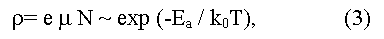
(here e is the charge of an electron, μ is an electronic mobility in the region of intrinsic conductivity, when concentration of carriers in a conductive zone grows with temperature due to thermal activation according to exponential law:
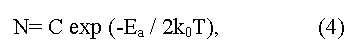
here C is a constant depending on parameters of conductive and valence zones, ko - L.Boltzmann constant, T - absolute temperature, Ea = (Eg/2) is an energy of activation (the factor 1/2 shows that Fermi level should be located in the middle of the forbidden gap). The method gives Eg value appropriate 0 K, and demands the account of temperature dependence of electronic mobility μ. In the case of semiconductors with low electronic mobility (in particular, the semiconductors having narrow on width d-zones) the activation energy Ea, determined from temperature dependence of electrical resistance, does not determine the real Eg value in a material.
The Eg value can be determined also by measurement of dependence of Hall factor [15] in intrinsic conductivity region using a formula:

here R is Hall factor, T is absolute temperature.
The frequent mistakes of Eg determination by the specified methods are due to: 1) unattainability of the region of extrinsic conductivity, influence of impurity levels activation and impurity contribution to conductivity; 2) failure to take into account the temperature dependence of mobility μ in the formula (3); 3) insufficient extent for the interval of temperatures ΔT used; 4) change of a chemical compound composition and homogeneity range at high temperature and so on [4,14,15].
The determination of Eg from edge of light absorption and from photo-conductivity of semiconductor is based on excitation of a valence electron into conductive zone due to absorbed energy of a photon. Direct (vertical) optical transitions (k2 = k1 + g, or k2 ~ k1, here k1 and k2 are wave vectors of an electron in a final and initial states, g is a phonon wave vector) and indirect (not vertical) optical transitions with phonon participation (k2 ~ k1+ Kph, here Kph is a phonon impulse) are possible. The edge of own absorption is determined for direct and indirect transitions accordingly by relations:
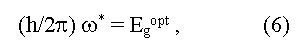
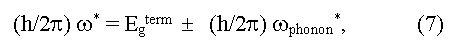
here ω* is a boundary frequency of absorption of photons, ωphonon is the frequency of absorbed (+) and emitted (-) phonons, Egopt and Egterm are optical and thermal widths of the forbidden zone. The equality Egopt = Egterm for direct vertical optical transitions follows from the expressions (6) and (7). In the case of indirect optical transitions Egopt may be as less (a case of phonon absorption) so more (a case of phonon emission) than the minimal distance between a valence and conductive zones (Egopt ≠ Egterm = Eg). In addition measured values of Egopt may essentially depend on crystallo-graphic directions in a sample [5]. Usually Egopt = Egterm in covalent crystals, Egopt > Egterm in ionic crystals, Egopt < Egopt for exciton absorption of light (formation of bonded electron and hole pares under light radiation). The exciton bandgap can be calculated from the equation:
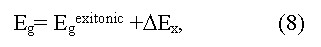
where ΔEX is an energy of exciton bonding (eV). Equations (6) and (7) are valid when Fermi level lies in the forbidden zone of a crystal. In high doped semiconductors of р-type (semimetals) the electron excitation into a conductive zone starts from Fermi level, being deep in a valence zone, thus the obtained Egopt value will increase up to Egopt ~ Egterm + EF. Optical methods of Eg determination in solids have the greatest accuracy (up to 0.001-0.0001 eV and more) and a wide range (up to several eV)] but sometime demand difficult interpretation of the peaks received [3,4]. In particular, some optical transitions may be forbid by quantum rules, following from symmetry of a crystal [4]. In result the observed optical peaks may correspond to tran-sitions of electrons not in extreme, but in others, distinct from them, points of Brillouin zone. The appropriate energy gap refer to as pseudo forbidden zones (direct, or indirect), which on occasion may differ from true Eg in some times [14]. The essential moment at the analysis of optical spectra is also to define the type of optical transition observed (direct or indirect). In particular, because of wrong interpretation of direct and indirect transitions some semimetals for a long time accepted for narrow bandgap semiconductors (Bi, Sb and other) [7,14].
Conclusion
Thus, the Egterm value (further called simply Eg) represents the true fundamental width of the forbidden zone of a crystal, undependent from crystallographic directions, that is responsible for all physical and physical-chemical processes connected with thermal activation of carriers in samples. At the same time, Egopt value though is connected with Egterm but has slightly smaller generality. Namely Egopt describes optical transitions of electrons in crystals at certain conditions of experiment (crystallographic directions, frequencies and polarization of optical phonons, type of optical transitions (direct, indirect) etc.). From here it follows, that it is possible to speak about reliable knowledge of Eg value only in case of comprehensive investigation of materials.
All reasons mentioned above were taken into account at design of the present Database covering values of width of forbidden zone Eg of the major classes of inorganic compounds. Database "Bandgap" contains information from basic Russian and foreign handbooks and papers. The methods of Eg determination and the appropriate temperature ranges are indicated. The data on chemical and phase composition of materials, type of a crystal lattice (system, structural type, space group), orientations of samples at optical measurements are given in addition. All given data correspond to mechanically free samples, normal atmospheric pressure and gravitation, absence of detectable external electric and magnetic fields.
Designations:
- ΔE - width of a forbidden zone (bandgap);
- Optical - the bandgap is determined from optical data;
- Thermal - the bandgap is determined on thermal activation of conductivity;
- Electrical - the bandgap is determined from electrical measurements;
- Photo. - the bandgap is determined from photoconductivity;
- Exciton - the bandgap is determined from optic exciton analysis;
- Theoretical - a theoretical estimation;
- h.t. - high temperature;
- RT - room temperature;
- l.t. - low temperature;
- KI, KII, KIII - various polymorphic modifications;
- (.) X, (.) Γ - various points of Brillouin zone;
- (//a, b, c), (E//a, b, c) or (A, B, C) - the vector of an electric field of the polarized light wave is parallel to crystallographic axes a, b, c, accordingly;
- (|− a, b, c), or (E |− a, b, c) - the vector of an electric field of the polarized light wave is orthogonal to crystallographic axes a, b, c, accordingly.
Literature:
[1] Wilson A.H. The Theory of Metals, Cambridge, 1953.
[2] Peiers R.E. Quantum Theory of Solids, Oxford, 1953.
[3] Ziman J.M. Electrons and Phonons, Oxford, 1960.
[4] Kittel C. Quantum Theory of Solids, New York, 1963.
[5] Blatt F.J. Physics of Electronic Conduction in Solids, New York, 1968.
[6] Harrison W.A. Solid State Theory, New York, 1970.
[7] Lovett D. Semimetals and Narrow Bandgap Semiconductors, London, 1977.
[8] Mott N.F., Davis E.A. Electron Processes in Non-crystalline Materials, Oxford, 1979.
[9] Amorphous Semiconductors, Ed. Brodsky M.H., Berlin, 1979.
[10] Cutler M. Liquid Semiconductors, New York, 1977.
[11] Kao K., Hwang W. Electrical Transport in Solids, Oxford, 1979.
[12] Mott N.F.Metal-Insulator Transitions, London, 1979.
[13] Regel A.R., Glazov B.M. Periodical Law and Physical Properties of Electronic Melts, Moscow, 1978 (in Russian).
[14] Ormont B.F. Introduction to Physical Chemistry and Crystall Chemistry of Semiconductors, Moscow, 1973 (in Russian).
[15] Bush G, Vinkler U. Bestimmung der Charakteristischen Grossen Eines Halbleiters, Ergebnisse der Exakten Naturwissenschaften, Bd.29, 145, 1956.
[16] Tsidilkovskiy I.M. Band Structure of Semiconductors, Moscow, Nauka, 1978 (in Russian).
[17] Fridkin B.M. Ferroelectrics-semiconductors, Moscow, Nauka, 1976 (in Russian).
[18] Bugaev A.A., Zaharchenia B.P., Chudnovskiy F.A. Insulator to Metall Phase Transition and its Applications, Leningrad: Nauka, 1979, 183 pp. (in Russian).
Dr. Mikhail A.Korzhuev